(One of the most complex/time consuming repairs I’ve done – so a very detailed write-up!)
Part 1
The board initially showed no signs of life with most TTL on the board not active at all. Digging deeper showed there would be tiny pulses of activity then nothing for a few seconds, then repeat, so it seemed a watchdog was constantly trying to reset the CPU. This was confirmed on the /RESET line of the CPU which was being pulled low for a period then released high as expected. Voltage to the CPU was good, as were the clock signals (the TMS34020 takes two clocks, one regular CPU, one ‘video’ clock).
The first thing the CPU is meant to do on reset is to fetch the reset vector from program ROM so it can start executing code. So examining the program ROMs showed the address lines were all pulsing at reset as if the CPU was trying to read, but the ROMs never output any data. The reason why no data was output is because the /OE (output enable) line is never set. There are no schematics available for this game, so to figure out why requires a lot of tracing and reverse engineering. Time to go deep..
Program ROM /OE is driven from pin 19 of the programmable GAL chip at U144. I dumped the GAL to equations, and also did the same with the MAME dump – both match so I can rule out the GAL itself being bad. The equations are:
/o21 = i7 * i8 * /i9
/o20 = i23 * i7 * /f17 * i8 * i9 * /i10 * i14 * /i11
/o19 = i23 * i7 * /f17 * i8 * i9 * /i10 * /i11
f17 = i3 * /i4
o16 = vcc
/o15 = i7 * /f17 * i8 * i9
So the outpin on pin 19 (/o19) is a function of 9 different inputs. Ouch. Without knowing what they do yet, I can see that all except i10 pulse at reset. Time to trace where they all go, which is very time consuming with the tiny traces on this board.
i7-i9 are effectively bits 29-31 of the CPU address bus (they get latched into the LS373@U139 first). It makes sense these bits are involved, because if we reference the memory map from MAME – those top 3 bits are used to identify each ‘section’.
static ADDRESS_MAP_START( main_map, AS_PROGRAM, 16, btoads_state )
AM_RANGE(0×00000000, 0x003fffff) AM_RAM
AM_RANGE(0×20000380, 0x200003ff) AM_READWRITE(main_sound_r, main_sound_w)
AM_RANGE(0×20000400, 0x2000047f) AM_WRITE(misc_control_w)
AM_RANGE(0×40000000, 0x4000000f) AM_WRITENOP /* watchdog? */
AM_RANGE(0×60000000, 0x6003ffff) AM_RAM AM_SHARE(“nvram”)
AM_RANGE(0xa0000000, 0xa03fffff) AM_READWRITE(vram_fg_display_r, vram_fg_display_w) AM_SHARE(“vram_fg0″)
AM_RANGE(0xa4000000, 0xa43fffff) AM_READWRITE(vram_fg_draw_r, vram_fg_draw_w) AM_SHARE(“vram_fg1″)
AM_RANGE(0xa8000000, 0xa87fffff) AM_RAM AM_SHARE(“vram_fg_data”)
AM_RANGE(0xa8800000, 0xa8ffffff) AM_WRITENOP
AM_RANGE(0xb0000000, 0xb03fffff) AM_READWRITE(vram_bg0_r, vram_bg0_w) AM_SHARE(“vram_bg0″)
AM_RANGE(0xb4000000, 0xb43fffff) AM_READWRITE(vram_bg1_r, vram_bg1_w) AM_SHARE(“vram_bg1″)
AM_RANGE(0xc0000000, 0xc00003ff) AM_DEVREADWRITE(“maincpu”, tms34020_device, io_register_r, io_register_w)
AM_RANGE(0xfc000000, 0xffffffff) AM_ROM AM_REGION(“user1″, 0)
ADDRESS_MAP_END
As an example you can see output 21 on the GAL has this equation:
/o21 = i7 * i8 * /i9
So if i7 is set (0×20000000) and i8 is set (0×40000000) but i9 is NOT set (0×80000000) then the resulting address is 0×60000000 which means ‘nvram’ is being accessed in the map.
Back to output pin 19.. i3 and i4 are effectively address bus bits 2 & 3 (latched via ls373@u7). i11 goes straight to pin 8 on the CPU which is /RAS. i10 goes to CPU pin 133 which is ‘/TR /QE’. So if we refer back to the equation:
/o19 = i23 * i7 * /f17 * i8 * i9 * /i10 * /i11
For /o19 to be low (and enable the program ROM) we need the address lines to be correct, /i11 (RAS) to be low which it always is, but also ‘/TR /QE’ to be low, which always measures as high. The manual describes ‘/TR /QE’ as ‘Transfer/output-enable. During a local-memory read cycle, TR/QE
functions as an active-low output-enable to gate from memory to LAD0–LAD31.‘. So it makes sense it’s involved, it’s part of the cycle of reading, but why is it stuck?
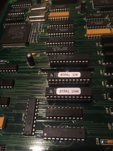
At first I thought the CPU had just failed internally – but there are some control pins that can affect the CPU state. The bus fault (BUSFLT) pin checked out ok, and the CPU wasn’t stuck in host mode (HCS pin). The smoking gun was a control pin called LDRY – this can halt the CPU in the middle of a memory cycle. This traced back to pin 21 of the GAL @ U11. Again, I worked out the equations for this GAL and started to trace what controls pin 21. The actual problem though was that this GAL had just failed and the outputs were garbage. Replacing this GAL fixed the LDRY input and the CPU finally started to read from the ROMs!
Part 2
So despite the CPU seeming to be running the game was still stuck on a black screen and resetting every second or so. The CPU was definitely running some code at least as video sync was now working (I assume the CPU sets up the video output). I then spent a lot of time tracing all the data and address lines, and found no problems. Eventually I decided to try and disable the watchdog after noticing the game in MAME takes a couple of seconds on a black screen before booting up and the pcb seemed to reset after only one second.
The watchdog/CPU reset is controlled by an IC called LTC690 at U83. A logic probe didn’t show anything wrong with this – there were occasional writes to reset the watchdog, but probably not as many as there should have been. The datasheet states the watchdog can be disabled (but the CPU reset functionality kept) by floating the watchdog input. So without much to lose I just cut the trace (pin 6). And the game worked!

I have no idea why the watchdog circuit has failed – but it’s arguably not needed as the watchdog is really just to protect against software faults and keep a machine running, so there’s nothing wrong with leaving this disabled for a ‘home’ pcb.

Part 3
On the home straight now – graphics and inputs fully working, but no sound. Sound comes from the BSMT2000 custom chip – a logic probe showed it had a clock input but no activity on the data or address bus. I was hoping the fault was that it was not receiving any data from the Z80 rather than having failed itself as I had no replacement. The Z80 memory map is controlled by a GAL like the main CPU. As before I dumped the equations from the MAME version which showed what outputs were in use. With this info and the logic probe it was pretty clear to see the GAL inputs were working, but the outputs were all stuck. I piggy-backed a replacement GAL and sound worked! So indeed the fault was that the Z80 was unable to write data to the BSMT2000.

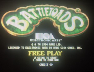
The bad GAL was desoldered and the replacement installed and the board was back to 100%.













Recent Comments