BryanMcPhail.com

Professional software development, amateur BMW tinkering, old arcade game stuff

By

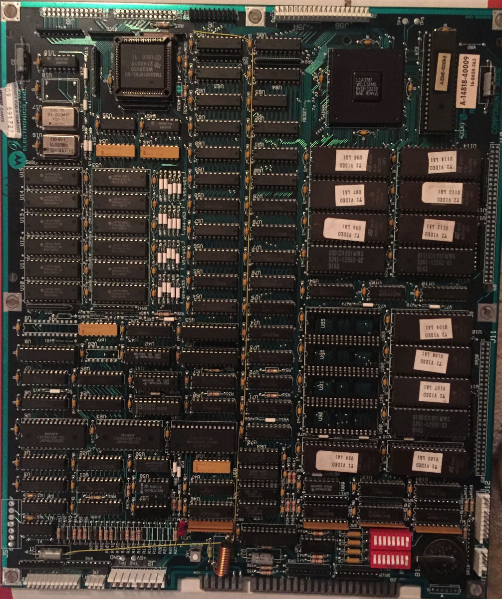
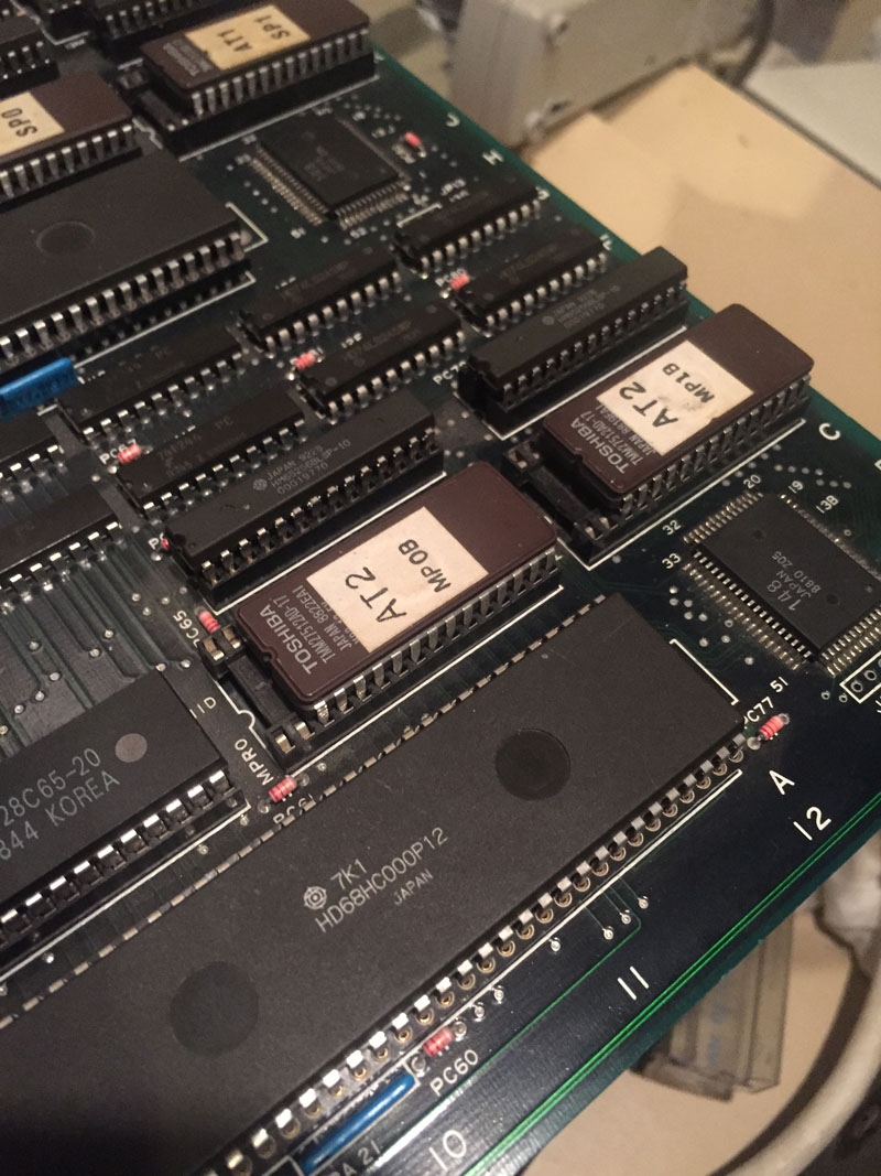
Konami Hyper Olympic bootleg arcade pcb repair

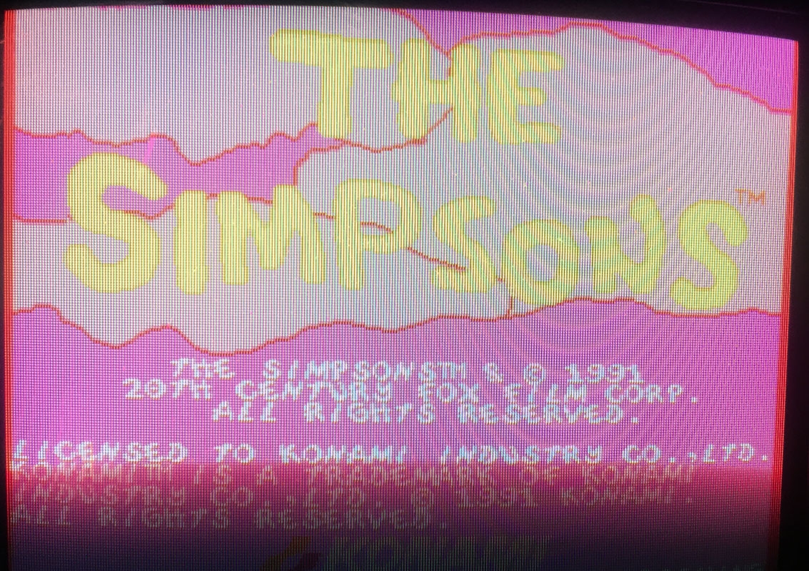
This board worked but had a strange magenta outline around the characters.  This was a very time consuming repair for what seemed a little fault, it didn’t help I started down the completely wrong path..

IMG_8079

IMG_8317

What wasn’t the problem

The eproms and color prom all tested good – so it wasn’t a simple case of corrupt data.  I’ve talked in many repair logs about pairs of sprite line buffers, which are present on this board as many others.  Because the magenta outline was present on all scanlines, this meant the problem had to be after the eproms (where the sprite data is sourced) but before the split into the two line buffers OR after the two line buffers are recombined before reaching the color prom.  So this cuts the potential problem chips right down – the eprom data goes to a bunch of 4 LS194 shift registers, which feed into the two sprite RAMs.  The data leaving the RAM travels to a LS273 then a LS157 which recombines into a single data stream (which goes to the LS258 which acts as the priority selecter by picking between either a sprite pixel going to the color prom or a tilemap pixel).

However, every single chip tested good, so this theory ended up being a complete waste of time.

What was the problem

The clue came when I forced the color prom to display only tilemap colors or only sprite colors (you can do this by forcing the top address line of the colour PROM either high or low – as per OBJOUTD at pin 14 on the schematics).  With the sprite palette forced on the sprites were 100% correct – after checking the palette in MAME I finally understood the fault – the ‘first’ pixel of the sprite was using the tilemap palette, as the magenta only existed in the tilemap palette and was being used instead of the dark brown expected by the sprite.

IMG_8327

IMG_8336

So why could that be…  In the schematics you can see OBJOUTD controls the prom switching between tilemaps and sprites, but the OBJOUT signal controls the data switching.  A LS174 makes the OBJOUTD and you can see it’s generated 1 CLK later on from OBJOUT.  Why I have no idea..  I didn’t find any problem there so I just patched OBJOUT to drive the prom directly – and this made the magenta outline appear on the right side, rather than left.  So instead of the prom palette being a pixel behind it was now a pixel ahead.  So it was as if the switch happened ‘half a clock’ out of time which is pretty weird.

IMG_8334.

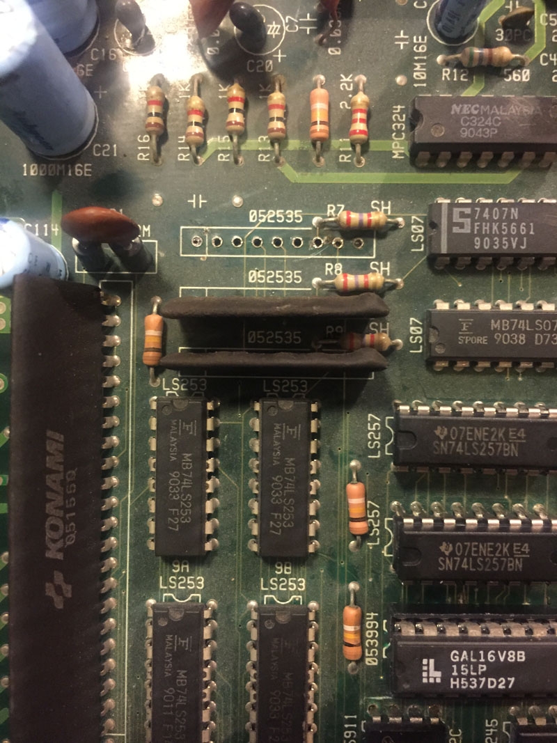
I examined what drove the CLK1 and /CLK1 signals which was an LS368.  On the original Konami board a custom chip drives the LS368.  However, on the bootleg was a weird hack involving two capacitors on the clock input line – one was damaged and removing it made the graphics perfect!  Not altogether uncommon to see hacks like this on a bootleg (a capacitor delaying a clock, in this case by ‘half’ or inverted phase) but not easy to find.

IMG_8330

IMG_8340


By

Konami Track And Field arcade pcb repair #3

Board booted to a screen full of zeroes which is an indication the CPU is running the start of the program at least (if not the screen would be full of random garbage rather than a consistent pattern).  Checking the eproms on PC found a couple were bad (inconsistent reads) but the main problem was the RAM chip next to the eproms was dead.  The part number is scratched out but it’s just a regular 6116 style RAM.

IMG_8068

IMG_8069

With that replaced the board booted to the title screen – but with obviously bad sprites in both the tile index and the Y position on screen.  The game also reset before entering gameplay, so definitely still a CPU/RAM related problem.  There are schematics available for this game, which show the custom chips used for sprite processing.  This board however, didn’t use any custom chips but instead had little daughterboards with regular TTL chips.  This is actually quite common in all of the Centuri licensed boards I’ve seen – probably there was a manufacturing shortage of the custom chips and the daughterboards were put in to meet demand.  I set about removing the daughterboards for test (the board should run without crashing, just no sprites, with them removed) and the board ran fine.  I then ran the board with the daughterboard sitting in the desoldered holes – and it ran 100% fine with working sprites!  It kept on working with the board soldered back on and a long soak test.  Very strange, I can only guess there was some kind of solder bridge short on the board somewhere, and the act of applying heat to remove the daughterboard cleaned it up.

IMG_8072

IMG_8173

Finally bad inputs were fixed by replacing a smashed resistor pack with one from a parts board.

IMG_8073


By

Midway Terminator 2 arcade pcb repair

Game was initially dead with video or sound output.  The TMS34010 CPU is the fore-runner of the CPU used in my earlier Battletoads repair and shares most traits with it including control pins that can halt the CPU for external memory access.  The logic probe showed a very similar problem to Battletoads initially – the CPU was resetting properly, getting a clock signal, but had no activity on the data/address bus.  Something was holding the LRDY (local ready) pin low so the CPU appeared to be in a wait state for something external.  That something was traced to the Intel security chip which is not replaceable if it has failed.  Luckily it hadn’t failed – the problem was that chip was not getting a clock signal so it was also stuck causing a deadlock.  I checked with the schematics and found the clock signal for the Intel chip came from…  the TMS34010 CPU.  This CPU actually provides clock outputs as well as having a clock input and it seemed this part of the CPU die had failed – a replacement CPU taken from a Mortal Kombat 2 board got the board to boot to the test menu, albeit unstable and crashing after a few seconds.  (The MK2 pcb failed to boot with the T2 CPU proving the CPU itself was bad).

IMG_8355

Finding the instability took much longer…  there was a previous repair to the board with 4 RAM chips replaced.  These all share a common data and address bus but a continuity check showed 2 chips had a couple of unconnected data lines – the soldered pins were not making good contact with the traces/thru-holes (specifically traces on the top side of the board rather than solder side).  With the solder reflowed the board was 100% again.

IMG_8353

IMG_8351 IMG_8359


By

Konami Simpsons arcade pcb repair

Board would not boot most of the time – when it did the check screen showed an EEPROM error as well as a ROM error.  The background of the check screen was also red when it should be black.

The EEPROMs on Konami games are known for failing, but a check with a logic probe and multimeter here showed that 5 of the 8 pins weren’t even connected – trace damage where the chip met the pcb.  With that repaired it made absolutely no difference to the boot failures or bad check screen.  In fact the logic probe showed the software wasn’t even trying to read the EEPROM as the chip select or clock pins never pulsed.  After checking the chips involved with reading the EEPROM data (shown in the schematics as EEPDI, EEPCLK, EEPCS) were fine I suspected the PAL chips used to form the memory map may have failed in a subtle way and were responsible for both the EEPROM error as well as the ROM one.  This was a fault I had encountered in the previous Konami Vendetta repair – the PAL worked enough to boot the game to the check screen but failed in some kind of edge case that would give bad output over certain memory regions.  Simpsons has two PALs like this – marked as 55394 and 55395.  55395 is the one that directly enables the EEPROM, but replacing this made no difference.  Replacing 55394 though finally enabled the game to boot properly with no errors – so the fault was most likely that it was activating regions at the wrong time.

IMG_8083

IMG_8081

The game still had a fault with the red channel stuck on, as well as not booting most of the time.  As I knew the palette RAM was ok (because of the game self test) I started with the custom 052535 DAC IC.  Replacing this made no change, I should have paid more attention to the schematics as there was also a LS273 chip in between the palette RAM and the DAC and this had simply failed with outputs stuck high.

IMG_8090

IMG_8091

IMG_8087

Inconsistent boot faults can be much harder to track down though – in this case I got a clue it was a physical problem when I found it would boot if I flexed the PCB a certain way.  Reflowing the solder on the surface mount custom ICs made no difference but removing all the ROMs and cleaning the ROM sockets did – one program ROM socket had a strangely dirty pin even though all the others were fine.  Game now booted and ran 100% of the time.

IMG_8274

By

Capcom CPS1 arcade pcb repair

Well, really a non-repair in some ways, but an interesting case to look at.

IMG_8057 IMG_8056

This board had a glitch in the background graphics – with repeated sections and blank sections.  The components involved are the custom CPS chip that generates the background, the RAM chips, the main CPU and any latches in between.  The data is written to RAM from the CPU through two LS245 latches(the red path), then the graphics chip reads from RAM through another two LS245 latches (the green path).

IMG_8367

You can rule this out being a RAM fault – because the RAM is paired, so it would need two different chips to fail in the exact same way which is unlikely (if only 1 chip failed then you would have bad tiles/colors not good tiles in the wrong place).

You can rule this out being a CPU fault because of the repeated data – the CPU can’t write one thing and have it go to different places at once in the RAM.  The RAM only accepts one address at once.

For the same reason the LS245 latches in between the CPU and RAM must be ok, they couldn’t cause a ‘repeat’.


So this must be a fault in how the graphics chip is reading the RAM (an addressing problem).  Initially I hoped for an easy fix as a broken trace on the board would cause this exact problem (with an address line broken the same data would be read at multiple addresses).  However the traces all run on the top of the board where a scratch is unlikely, and everything was perfect.  A multimeter confirmed continuity all the way from the graphics chip to the latches to the RAM (it also confirmed it to the top B board but I knew that wasn’t at fault as I had already tried out a known working B board).

I ‘mocked up’ the problem in the MAME debugger.  By forcing RAM line 0×400 (or something) to always be low I repro’d the problem (this means that data at say 0×600 reads the same as data as 0×200 (the ’4′ is masked low), 0×602 same as 0×200, etc.  So 1 bit was stuck low in either the LS245 latch, or the CPS-A-01 graphics chip itself.  Removing surface mount chips via hot air is quite easy – replacing them is much harder…  but eventually both were replaced with others from a parts board – and the exact same fault remained :(   That means the fault was definitely within the unreplaceable CPS-A chip (well, you could replace it with another from a working board, but much easier just to use that board).

And in this case, that’s what I did – an A board from a Magic Sword with no sound and bad B board was swapped in to keep the SF2 World Warrior working.

No Sound fix

A logic probe showed the audio Z80 CPU was running, so I examined the analog audio output by attaching a pair of power speakers at various points on the board.  At first the op-amp at IC138 (pins 1, 2 and 3), then the volume control (VR1), then inputs to the power amp @ 16A.  Faint sound was heard at all points so the power amp was likely the problem.  The amp was removed from the board with the dead CPS-A and soldered in to give a fully working SF2 World Warrior.

IMG_8147


By

Capcom Ghosts n Goblins arcade pcb repair

This looked like an easy fix, but ended up taking a very long time indeed…  The fault was obvious – every second scanline of sprites was missing.  As I’ve talked about on previous posts most games use a pair of line buffer circuits – whilst one is written to by the graphics hardware, the other is read out to the screen.  I was able to confirm what one was broken by shorting data pins on the RAM – one corrupted the visible parts of the sprites, the other had no effect at all.  So the one with no effect was the one that wasn’t producing any data to the screen.

IMG_8032

Ghosts N Goblins uses a fairly unusual RAM chip for the line buffer – the type is scratched out on the chip but schematics show it is a 20 pin CXK5808P.  This seems quite hard to obtain now-a-days – luckily the board was designed that a regular 6116 slimline RAM could be used instead.  As the logic probe didn’t show any problems with the surrounding IC’s I assumed the RAM was bad and swapped it out for a fresh 6116.  And.. the fault was still there.

IMG_8028

More work with the logic probe showed that the LS257 at 7L had pulsing inputs, but the outputs were always high.  That must be the fault right?  Well, it was removed and tested fine, and any replacement acted the same on the board.  This chip at 7L is how sprite data gets into the line buffer circuit.  On the next clock the data goes around to the LS21 at 14L – this is the transparency check – all high inputs indicate it’s a transparent pixel for the sprite that should not be written to line RAM.  Any low indicates it’s an opaque pixel that should be written.

IMG_8102

My next approach was to use a dual input oscilloscope – putting one probe on the good line buffer, and the other at the equivalent point on the bad line buffer.  This really just confirmed that everything seemed to be working fine and the problem was no data was getting that far on one buffer only.  Another hint this part of the board was ok was that I could force some of the input pins to GND and correctly saw ‘solid’ color blocks on screen (as opposed to a block with every second line missing).

IMG_8098

After a lot of wasted time I went back to the start of the schematics and found there is another place where the sprite data splits into two paths – 11F and 12F split the ‘DE’ bus into ‘DEA’ and ‘DEB’ and it was the LS245 feeding DEB that had failed, with all outputs stuck high.  With this one IC replaced, everything was 100% again.

IMG_8182

IMG_8193

IMG_8261 IMG_8265 IMG_8267

By

Namco Assault arcade pcb repair

(aka Atari Assault, as it was licensed to Atari for the USA).

Board would boot up and sometimes say DRAM error, but most often would not boot properly at all and just constantly reset.  I used the MAME debugger to confirm any error with the main CPU RAM causes the DRAM error message.  The nice thing about this pcb is all the RAM is in sockets from the factory – so very quick to swap out main RAM for spares.

IMG_8178

This indeed fixed the DRAM error and sometimes the game would play perfectly – but still sometimes it would not boot at all.  As so many things are in sockets on this board I removed everything I could and cleaned the pcb and all sockets – Simple Green and paintbrush then rinse with water.  PCB looked as good as new!  Even better it booted 100% of the time with everything replaced.

IMG_8285 IMG_8288


By

Data East The Real Ghostbusters arcade pcb repair #2

Board was completely dead to start with – no video or audio output.  The video board from Gondomania is the same as the Ghostbusters video board so I started off by attaching a known working video board to the Ghostbusters top board.  This gave me some garbage video:

IMG_8412

Which confirms there were faults on both the Ghostbusters top CPU board (because the software was not running) and the bottom board (because there was no video output at all).  The top board was an easy fix – the CPU was inserted backwards – luckily it wasn’t damaged and the game ran fine when reinserted properly.

To debug the bottom video board I started by examining the signals going to the connector between the two boards.  Surprisingly the video sync (CRTSYNC) and vertical blank (VBLK) all pulsed correctly on a logic probe which confirmed the video clock was working as well as the custom IC that drives sync.  The RGBBL (RGB blanking) signal though was stuck low and this seemed to inhibit any RGB output.

IMG_8420

From there it was just a case of tracing back all the inputs to RGBBL until a problem was found – which was the HCLK0 input was stuck high.  Rather strangely this turned out to be a physical problem on the board rather than a TTL one – the leads on some of the ICs had not been clipped short enough and at one point on the board the HCLK line was shorted to a +5V line.  When cleaned up everything worked 100%.

IMG_8427 IMG_8429


By

Sega Super Monaco GP arcade pcb repair

Super Monaco GP!  Same board as Afterburner, one of the classic late 80′s sprite scaling boards.  Very complex hardware with 2 68000 CPU’s + Z80 for audio.  When powered up this board would flash the screen for a second and then sit dead on a black screen.  Logic probe showed the main 68000 was getting a clock signal but there was no activity on any data or address pin.  The probe also revealed the reset logic was working fine, and there was a burst of data activity for a second or less at boot up before it stopped.

IMG_7856

A stopped 68000 usually means there is a bus error or illegal instruction and the CPU has crashed, usually asserting the bus error hardware pin.  In this case the BERR pin didn’t show anything.  I suspected the software was actually issuing a STOP command and indeed when I fired up the MAME debugger I found all the exception handlers jumped to STOP routines.  So the theory was the program started to run, crashed, then the CPU was told to stop.  The most common reason for a crash would be bad RAM – because as soon as the program tries to return from a subroutine, a bad value would be returned by the RAM (most likely 0xffffffff) which would trigger a bus error for unaligned access.

Piggybacking known good RAM didn’t help so I decided to write a little diagnostic ROM that would print RAM values to screen.  The program itself is very careful not to use any RAM of course – so no subroutines, just logic instructions and static branches.  After trying the program out in MAME, I first needed to modify the board to run on 27c010 eproms – rather than the 27c1000 pinout eproms my programmer didn’t support.  Jumpers/resistors can be toggled to switch between the two different types (see Afterburner schematics for full details).  The program worked first time – which was great because it proved the main CPU was running as well as the palette and text layer hardware.

IMG_7864

Running the real hardware side by side against MAME showed a couple of bad bits in the 0×280000 range – which according to MAME memory map is actually the sub CPU RAM.  I used the logic probe to short pins on the RAM chips to identify what physical chip matched that address range and then piggybacked the known good RAM on top.  The values flickered and changed which is a good sign the RAM was bad (the flickering being the two RAM chips arguing over the correct value).  The RAM (TMM2063@IC31) was removed and replaced and the board worked 100% again.

IMG_7877

Diagnostic ROM and source is included below – note it’s a very quick hacky test!  Not something polished and easy to use.

IMG_7879

IMG_7878

IMG_7885

Diagnostic ROM and source – MakeSMGP- provided with no warranty

By

Capcom Last Duel arcade pcb repair

Game played but with lines through sprites and corrupt sprite colours.  Diagnosis was quick – it was clear a mask ROM was missing on the video board, and strangely it’s sister ROM was inserted with a pin outside the socket.

IMG_7982 IMG_7976

The board has pins for both a 23c2000 16 bit mask ROM or two 8 bit 27c301 ROMs, probably so the factory had flexibility to fit whatever type was cheaper during the production run.  But.. the 27c301 is a 32 pin IC, and the mask ROMs fitted are only 28 pin.

eprom_27301_pinout

This borrowed picture shows how it is possible – the top 4 pins are VPP (programming voltage), VCC (+5V), OE (output enable), PGM (enable programming).  The 28 pin mask rom doesn’t need the programming pins, and it omits OE in favour of just using CE (chip enable), so it always outputs when enabled.  The +5V line then just runs to the NC (not connected) spare pin on the 27c301.  So this way the board can use both the 28 pin or 32 pin ROM with no other modification.  In this case I used a fresh 27c301 and everything was fixed.

IMG_7988

IMG_7987  IMG_7991 IMG_7996