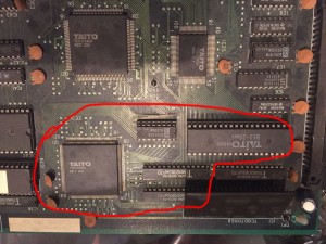
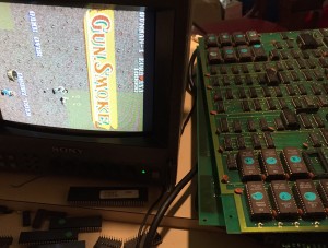
After making a custom loom for this untested pcb, I found it booted to garbage. Booting to garbage is at least better than not booting at all though as it shows the video output section is at least running. After checking the voltages at the chips were 5V (or slightly higher) and that the program eproms I examined other socketed chips and found the custom chip 34 had badly corroded pins when removed from the socket, and a few of the legs snapped completely.
Repair 1 – clean up the corrosion and mount the chip in a new socket and solder through from the broken pins to the socket top. Not the prettiest fix but it works.
Unfortunately, this didn’t change much with regards the corruption. So I put a logic probe on the CPU and found the clock pins (Q & E) and the address and data bus pins had activity on them. However, the read/write pin seemed stuck high – this means the CPU could only be reading from RAM, never writing to it and a CPU that can’t write data certainly can’t run properly. The CPU also got very hot very quickly.
Theory 1 – CPU has failed internally, and R/W has stuck high.
Theory 2 – the chip the R/W pin connects to has failed and forced the R/W line high regardless of what the CPU tries to do.
The CPU is in a socket so that’s the easiest thing to try first – however I didn’t own others of this type to swap in (HD6309, slightly different from regular M6809) so had to wait a week to order some from Ebay.
And.. didn’t help, no change. The R/w pin connects to an LS368 chip at location 5A and suspiciously it has corroded pins, even though all the chips around it are perfect. So remove and replace that.
And.. still corruption, though it’s different and it seems the CPU is definitely doing ‘something’ as the corruption cycles a few times before stopping. In retrospect I think the stuck R/w pin theory was a bit flawed – if it was truly stuck then the corruption would probably be random each time, and this was consistent. Instead more likely the CPU started to run the program then just parked itself in an infinite read loop when it detected a failure. The LS368 was probably bad in some other way though.
So Pacland in MAME shows that on boot the game should print 0 0 0 on screen to show all self-tests passed. The curious thing about the new corruption is you could clearly see the screen clear a few times then a couple of zeros appeared, just not where you would expect them to be.
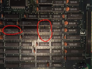
So new theory – RAM is bad – as when the CPU tries to write the zero character it gets reflected in a bunch of other locations (so the internal address decoding has failed). So, desolder and test the 7 6116 RAM chips on the top right of the board. The top 4 is the RAM for the tile maps, the bottom 3 is for the sprites and CPU workram.
Unfortunately, all the RAM tested good. So.. time to examine the schematics to see what is in-between the RAM and the CPU. I desoldered the IC’s at 10B, 9E, 9D, 10N, 9F – these control the enable lines to the RAM. All tested good so no progress.
Usually in arcade schematics you read from left to right – inputs on the left, and outputs on the right. There’s an exception in Pacland though, as the tile map ram chips can be addressed by the main CPU, or by the graphics hardware through a custom chip. So the address bus on the right of the RAM in the schematics is actually an input, and it comes from a pair of LS365 chips. These chips seems relatively rare on arcade pcbs, and my tester doesn’t support them. Their use seems to be in allowing both the CPU and graphics hardware access to the RAM chips. This is driven by the 2H signal – from the name I assume it toggles twice for every horizontal pixel – so for every pixel on the screen both the CPU and graphics get RAM access.
Switched these chips out for new – and instantly no more corruption! The 0 0 2 self test signals bad RAM, but this was expected as I hadn’t replaced the sprite ram at this point.
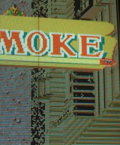
In game however, corruption remained on the backgrounds, but at least sprites and logic were working 100%! Time to look at the video part of the schematics which I’d mostly ignored until now. Custom chip 36 makes the tile maps. It has access to the tile map ram of course, two eproms with graphics data, and two color proms. We know the tile map RAM itself is good, so time to test the LS174 and LS86 chips that drive addressing to the graphics eprom. Unfortunately all tested good, so the problem wasn’t there.
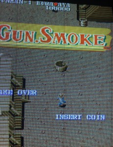
Tracing back further shows a LS365 and LS366 involved in addressing the tile map ram from the graphics side (NOT used by the CPU side access). Really I should have tested them first as having already found a bad LS365 there’s a good chance another from the same batch would have failed in the same way. Replaced these and everything was good!
Time taken : > 10 hours over 3 weeks (lots of waiting for parts to arrive)













Recent Comments